Project Overview
This project focused on the design and implementation of a fully functional 8-bit RISC CPU using SystemVerilog on an Intel MAX10 FPGA.
The processor supports arithmetic, logical, and memory operations, along with condition flags for signed and unsigned computations.
It was part of an advanced digital systems lab exploring CPU datapath architecture, hardware-level control, and instruction sequencing.
Repository 🔗
View Full Source Code on GitHub
System Architecture
The CPU was structured into modular hardware blocks that closely mimic the organization of a classic RISC processor.
Each module was independently designed, simulated, and then integrated into the full datapath.
// module organization and cpu i/o
module cpu_top (
    input  logic [9:0] SW,
    input  logic [1:0] KEY,
    output logic [9:0] LEDR,
    output logic [7:0] HEX0, HEX1, HEX2, HEX3, HEX4, HEX5
);
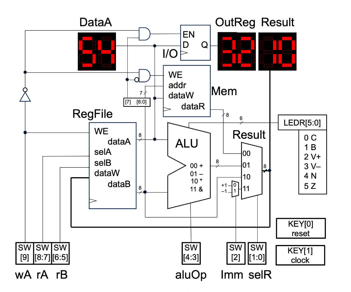
1. Register File
A dual-ported register file provides simultaneous read access to two registers (rA and rB) and write-back access through a third port (rW).
It consists of four 8-bit general-purpose registers, accessible via switch selection on the FPGA.
module register (
    input  logic [1:0] selW, selA, selB,
    input  logic [7:0] dataW,
    input  logic clk, reset, writeEnable,
    output logic [7:0] dataA, dataB
);
    logic [7:0] R0, R1, R2, R3;
    always_comb begin
        case(selA)
            2'b00: dataA = R0;
            2'b01: dataA = R1;
            2'b10: dataA = R2;
            2'b11: dataA = R3;
        endcase
        case(selB)
            2'b00: dataB = R0;
            2'b01: dataB = R1;
            2'b10: dataB = R2;
            2'b11: dataB = R3;
        endcase
    end

    always_ff @(posedge clk) begin
        if (reset) begin
            R0 <= 0; R1 <= 0; R2 <= 0; R3 <= 0;
        end else if (writeEnable) begin
            case(selW)
                2'b00: R0 <= dataW;
                2'b01: R1 <= dataW;
                2'b10: R2 <= dataW;
                2'b11: R3 <= dataW;
            endcase
        end
    end
endmodule
2. Arithmetic Logic Unit (ALU)
The ALU supports addition, subtraction, multiplication, and logical AND.
It outputs six condition flags to indicate overflow, carry, borrow, zero, and negative results for signed and unsigned operations.
module alu (
    input  logic [1:0] aluOp,
    input  logic [7:0] dataA, dataB,
    output logic [7:0] result,
    output logic [5:0] flags
);
    logic n, z, c, br, vp, vn;
    always_comb begin
        case (aluOp)
            2'b00: result = dataA + dataB;
            2'b01: result = dataA - dataB;
            2'b10: result = dataA * dataB;
            2'b11: result = dataA & dataB;
        endcase

        c  = (dataA[7] & dataB[7]) | (dataA[7] & ~result[7]) | (dataB[7] & ~result[7]);
        br = (~dataA[7] & dataB[7]) | (b[7] & result[7]) | (~dataA[7] & result[7]);
        vp = (~dataA[7] & ~dataB[7] & result[7]) | (dataA[7] & dataB[7] & ~result[7]);
        vn = (dataA[7] & ~dataB[7] & ~result[7]) | (~dataA[7] & dataB[7] & result[7]);
        n  = result[7];
        z  = (result == 0);
        flags = {n, z, c, br, vp, vn};
    end
endmodule
3. Immediate and Result Multiplexers
An immediate multiplexer selects between +1 (0000_0001) and -1 (1111_1111) when the Imm switch is active.
A result multiplexer controls the data written back to the register file, selecting from:
- Memory read data
- ALU result
- Register B output
- Immediate constant
This architecture enables flexible MOV, LOAD, STORE, and ALU instructions using a minimal switch interface.
4. Memory and Output Register
A simple addressable memory block (128 x 8 bits) stores data via dataA and dataB:
- When
writeEnable=0anddataB[7]=0, data is written to memory at addressdataB[6:0]. - When
writeEnable=0anddataB[7]=1, data is routed to the output register, displayed on the HEX2–HEX3 displays.
Instruction Set
The processor supports 8 custom instructions, each implemented through specific switch configurations:
| Instruction | Operation | aluOp | Imm | selR | Description |
|---|---|---|---|---|---|
ADD rA, rB |
rA ← rA + rB | 00 |
0 |
01 |
Arithmetic addition |
SUB rA, rB |
rA ← rA - rB | 01 |
0 |
01 |
Arithmetic subtraction |
MUL rA, rB |
rA ← rA * rB | 10 |
0 |
01 |
Multiplication |
AND rA, rB |
rA ← rA & rB | 11 |
0 |
01 |
Logical AND |
MOV rA, rB |
rA ← rB | 00 |
0 |
10 |
Register copy |
MOV rA, +1 |
rA ← +1 | 00 |
0 |
11 |
Increment register |
MOV rA, -1 |
rA ← -1 | 00 |
1 |
11 |
Decrement register |
STORE |
mem[rB] ← rA | — | — | — | Write to memory |
Testing and Validation
Each instruction was manually loaded via FPGA switches and clocked using push buttons.
To validate functionality, several programs were written directly in machine language, including:
- Summation Loop: Incrementing values and accumulating totals in memory.
- Factorial Computation: Iterative multiplication of decremented registers.
- Fibonacci Sequence: Memory-based recursion using register swapping.
- Greatest Common Divisor (GCD): Subtraction-based Euclidean algorithm.
Program correctness was verified through HEX display outputs and internal flag patterns on the LEDRs.
Hardware Demonstration
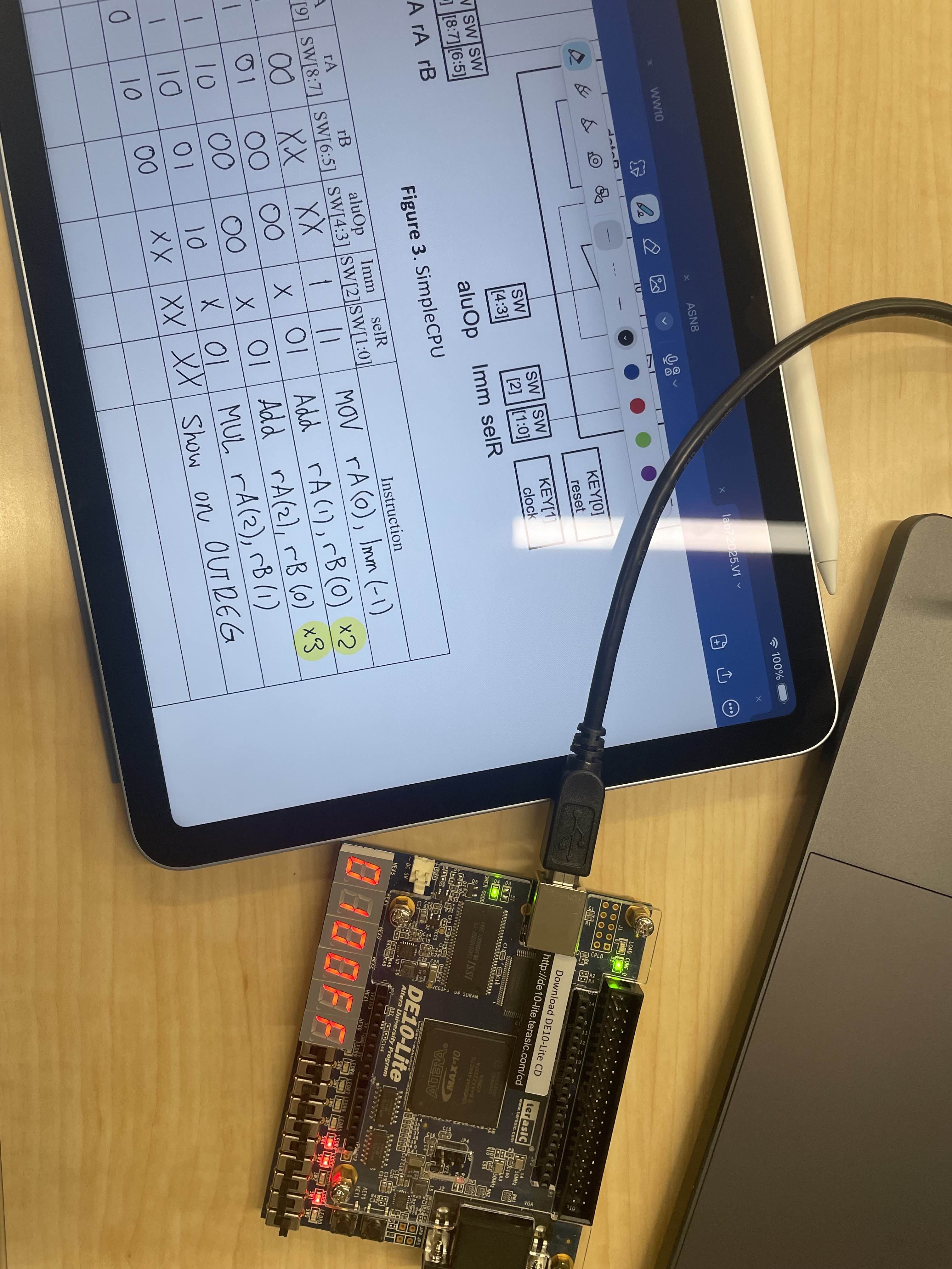
The CPU was deployed on an Intel MAX10 FPGA development board, with all inputs controlled by onboard switches and outputs displayed via HEX displays and LEDs.
Lessons Learned
- Designing at the hardware instruction level deepened understanding of datapath timing, flag propagation, and signed arithmetic behavior.
- Debugging FPGA clock synchronization issues required precise understanding of edge-sensitive logic.
- This project solidified the link between CPU architecture theory and digital logic implementation.