Overview
In an effort to learn PCB design in Altium, I gave myself the challenge of fully designing a board in a weekend. So I designed a mixed-signal telemetry node intended for automotive diagnostics. The system aggregates real-time data from GNSS/GPS, digital and analog thermal sensors, and Hall-effect speed sensors, transmitting packetized data to a central vehicle controller via the CAN Bus.
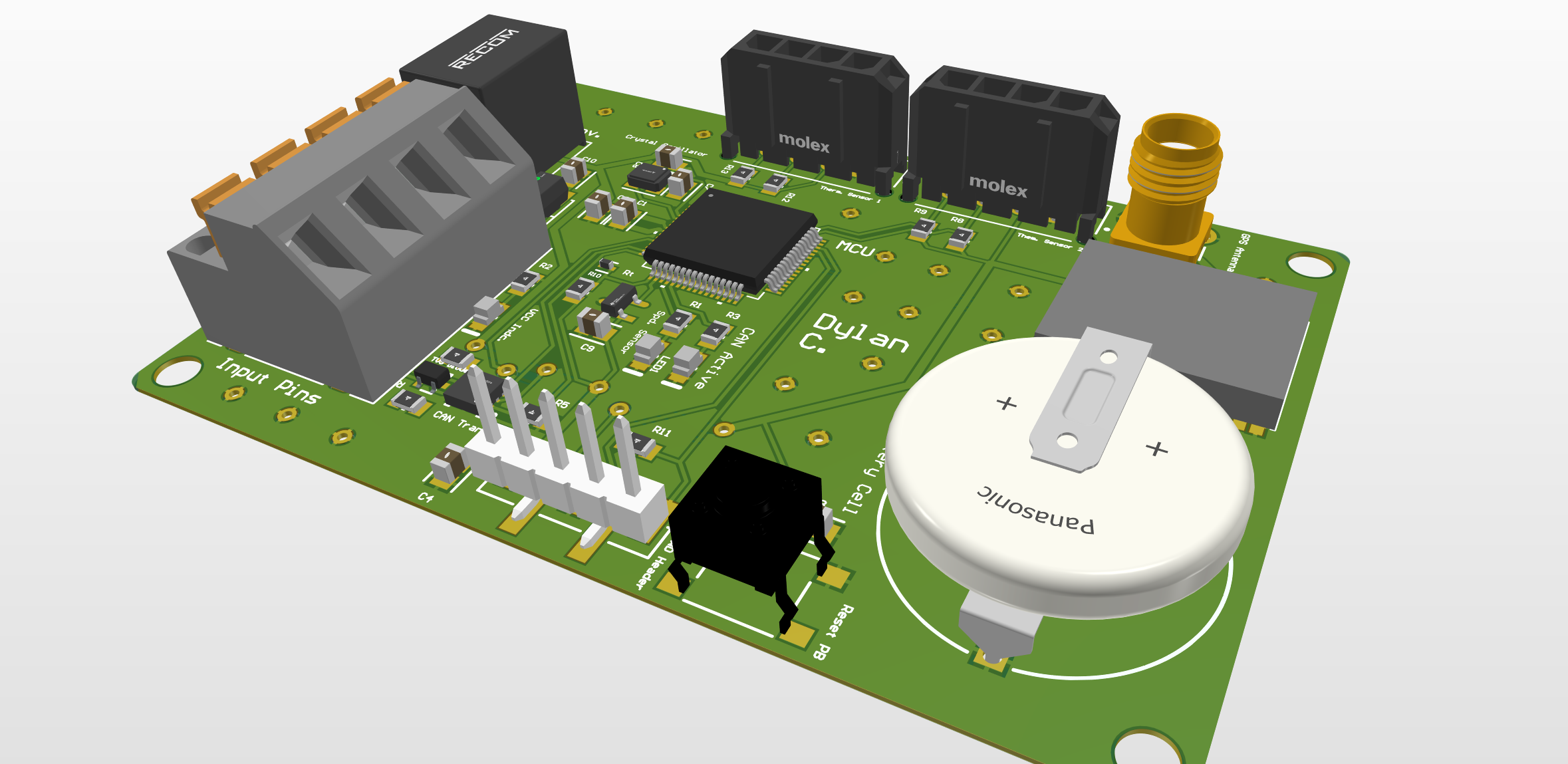 Figure 1: 3D Render of the Telemetry Unit designed in Altium Designer.
System Architecture
The core of the system is the STM32G0B1 (ARM Cortex-M0+) microcontroller. I selected this MCU for its rich peripheral set (specifically FDCAN and multiple USARTs) and low power consumption.
The system is partitioned into three distinct electrical zones to minimize noise coupling:
- High-Noise Power Area: Input protection and DC-DC conversion.
- Digital Logic Area: MCU, Crystal Oscillator, and Status LEDs.
- RF & Sensor Area: GPS/GNSS path and sensitive sensor interfaces.
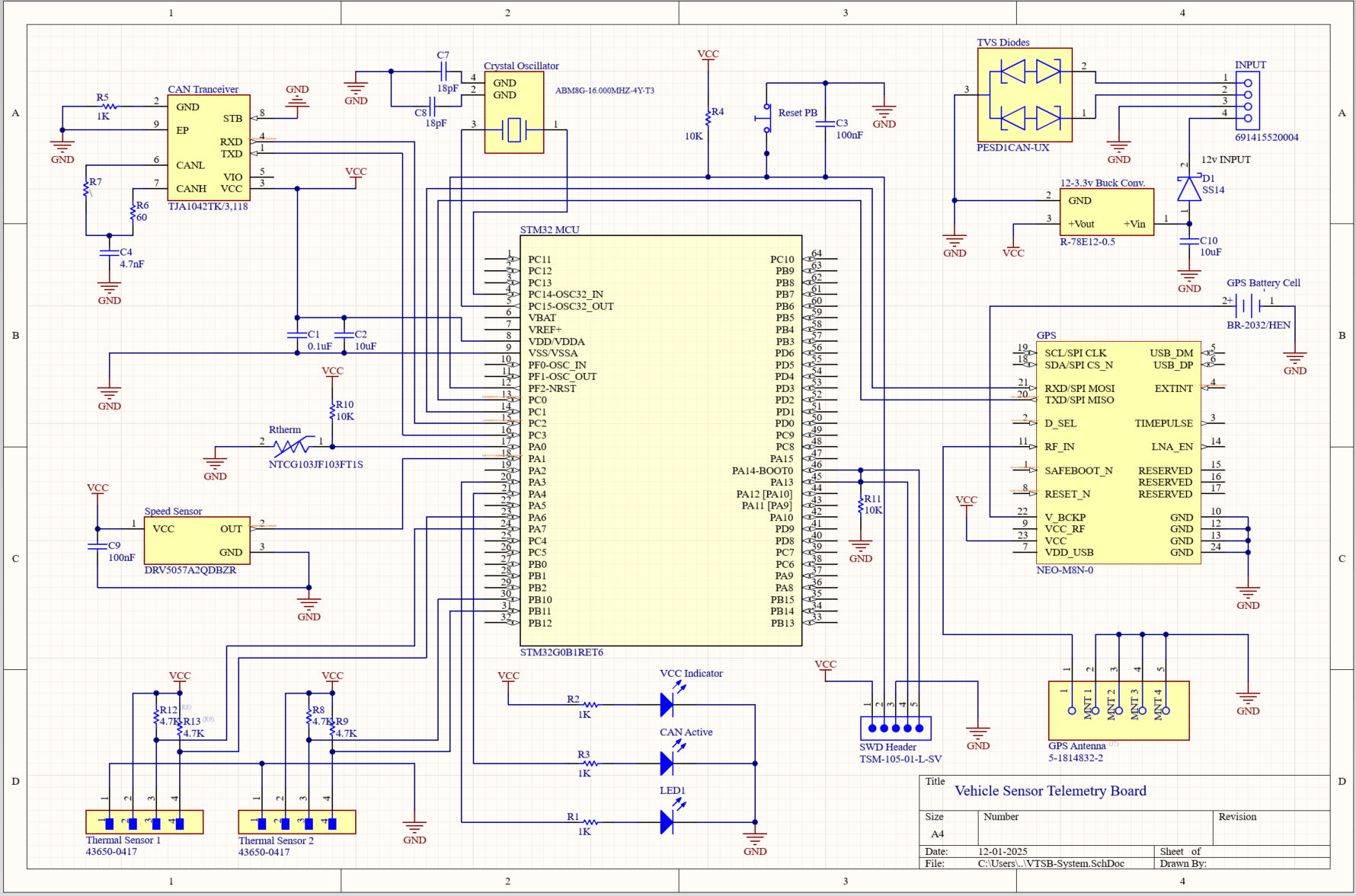 Figure 2: Complete schematic showing all parts of the board. I’ve since learned how to make the schematic cleaner using ports.
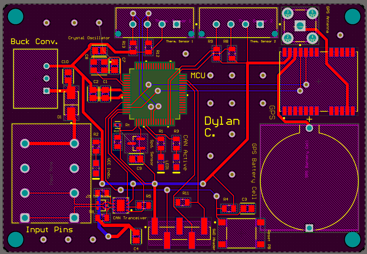 Figure 3: Complete System Schematic showing logical partitioning.
Key Engineering Challenges
1. Automotive Power Design & Protection
A standard vehicle 12V rail is noisy. To ensure the 3.3V logic remained stable during voltage transients:
- DC-DC Buck Conversion: Replaced inefficient linear regulators with a Switching Regulator (Buck Converter) to maximize efficiency and minimize heat.
- Protection Circuitry: Implemented a Schottky diode for reverse polarity protection (preventing damage during battery installation) and input bulk capacitance to filter noise.
- Loop Optimization: In the layout, I minimized the surface area of the high-current switching loop (input Cap > buck converter > diode) to reduce EMI.
2. High-Speed Differential Signaling (CAN Bus)
The communication backbone relies on a TJA1042 Transceiver. To ensure data integrity over long cable runs:
- Split Termination: Implemented a split termination network to improve noise rejection.
- Transient Protection: Added TVS Diodes immediately at the connector entry to shunt high-voltage spikes before they reach the transceiver.
- Differential Routing: Routed
CAN_HandCAN_Las a tightly coupled differential pair with length matching to ensure synchronization.
3. RF & Signal Integrity
For the GNSS (GPS) module, the signal path from the module to the SMA connector required careful attention. I routed the RF trace away from the noisy switching power supply and ensured a continuous ground plane reference on the layer beneath to maintain the necessary impedance.
I also integrated external connectors for the thermal sensors. Instead of relying solely on onboard sensors, I designed external I2C interfaces with local power and pull-ups, allowing the unit to monitor remote vehicle components (like battery cells) rather than just PCB ambient temperature. Additionally, there is an onboard thermistor to monitor the board temperature under operation located right next to the MCU and power area.
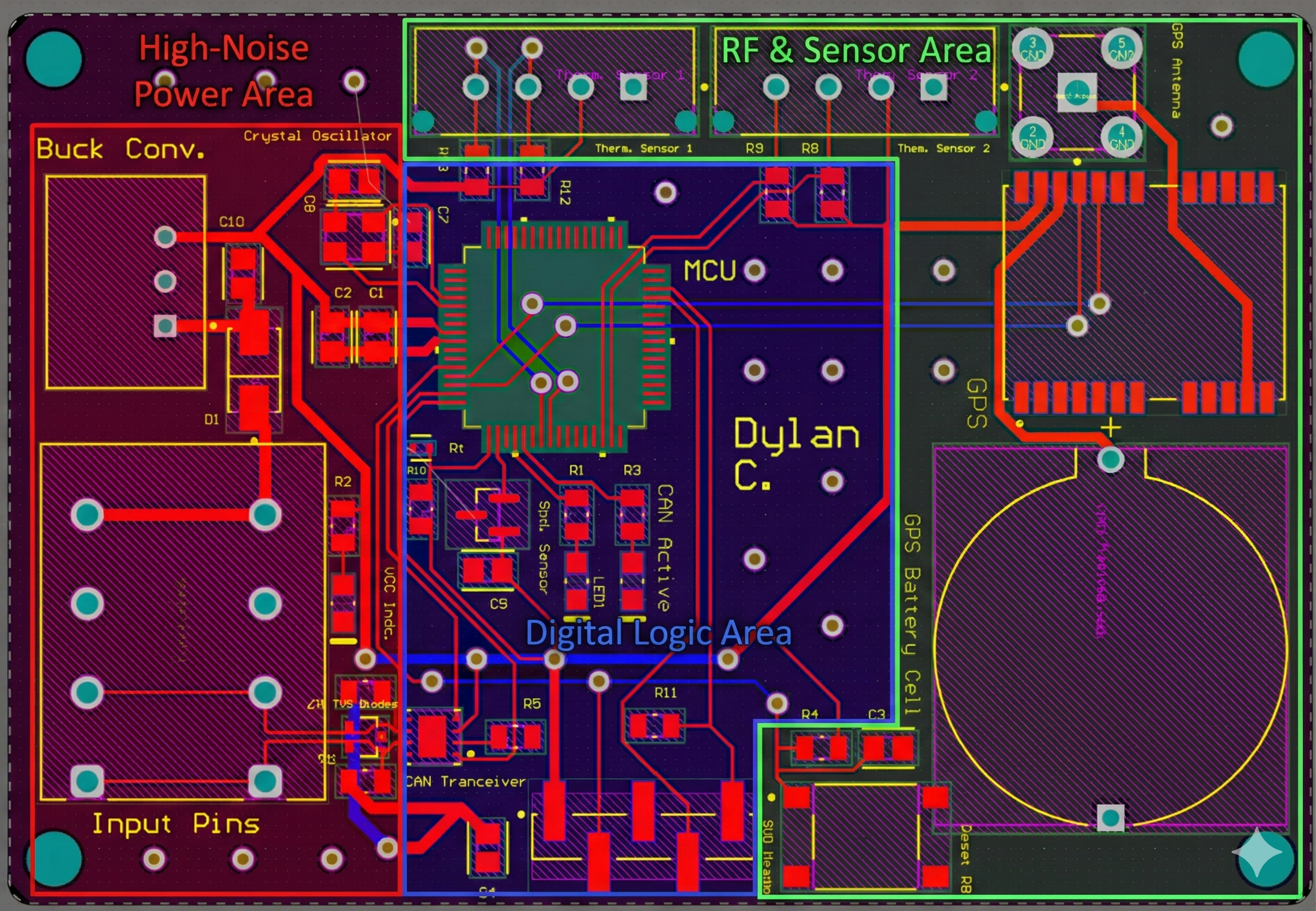 Figure 4: PCB Layout highlighting the strict zoning of Analog, Digital, and Power domains.
Result
The final design is a compact, 2-layer PCB routed in Altium Designer.