Overview
Measuring the speed of moving objects using a 10.525 GHz X-band radar module is fundamentally a mixed-signal hardware challenge. The radar transceiver outputs a raw Intermediate Frequency (IF) signal based on the Doppler shift. For standard speeds (0–100 MPH), this frequency shift sits squarely in the low audio range (tens of Hertz to a few kilohertz), but the amplitude is exceptionally weak—often in the microvolt range.
The objective of this project was to design a custom PCB from the ground up that could extract, cleanly amplify, and digitize this fragile analog sine wave while operating right next to a high-speed, noisy microcontroller.
To accomplish this, I engineered a complete hardware and firmware system:
- A 4-layer mixed-signal PCB designed in Altium Designer.
- An active analog signal chain simulated in LTspice utilizing rail-to-rail op-amps.
- A linear power distribution network dropping a 7.4V Li-ion source to a stable 3.3V logic rail.
- Bare-metal C firmware on an STM32G4 to sample the waveform, calculate velocity via DSP, and drive an OLED display.
System Flow
- Radar Module emits 10.5 GHz wave and outputs the low-frequency IF Doppler shift.
- Active Filter Stage removes high-frequency noise and applies ~175x AC gain.
- STM32G4 ADC samples the amplified 0–3.3V analog waveform.
- CMSIS-DSP Pipeline executes a Fast Fourier Transform (FFT) on a continuous DMA buffer to isolate the dominant Doppler frequency..
- Velocity Math converts frequency to speed.
- OLED Display updates the real-time speed via I2C.
Repository 📂
Full source code and manufacturing files:
Github Link
The Mathematics of Doppler DSP
To accurately extract velocity from a raw analog signal, the firmware cannot just rely on black-box libraries. The system must perfectly align the underlying physics of the microwave shift, the hardware timing of the STM32, and the mathematical resolution of the Fast Fourier Transform (FFT).
1. The Physics: Doppler Frequency Shift
The HB100 X-band radar module emits a continuous microwave signal at f0 = 10.525 GHz. When this wave hits a moving object, it reflects back with a compressed or expanded frequency. The radar module mixes the transmitted and received signals to output the difference—the Intermediate Frequency (fd).
The governing equation for this shift is: fd = (2 × v × f0) / c
Where:
- fd = Doppler shift (Hz)
- v = Velocity of the target (m/s)
- f0 = Transmit frequency (10.525 × 10⁹ Hz)
- c = Speed of light (2.9979 × 10⁸ m/s)
Rearranging this to solve for velocity gives us our fundamental DSP target. We need to isolate fd to find v: v = fd × [ c / (2 × f0) ]
2. The Time Domain: Sampling & Nyquist Limits
To perform an FFT, the STM32’s Analog-to-Digital Converter (ADC) must sample the waveform at a rigidly precise interval. I configured the system to sample at exactly fs = 10,000 Hz (10 kHz).
According to the Nyquist-Shannon sampling theorem, the absolute maximum frequency a digital system can measure is half its sample rate. fmax = fs / 2 = 5,000 Hz
By substituting 5,000 Hz back into our Doppler equation, we can calculate the physical speed limit of the radar: vmax = 5000 × [ (2.9979 × 10⁸) / (2 × 10.525 × 109) ] ≈ 71.2 m/s (256 km/h)
A 10 kHz sample rate perfectly blankets the expected speeds of terrestrial vehicles while keeping the DMA buffer memory footprint small.
To hit exactly 10,000 Hz, I configured STM32 Hardware Timer 6 to act as the ADC trigger. Running on a 16 MHz system clock, the hardware divider math is: ftimer = SystemClock / [ (Prescaler + 1) × (Period + 1) ] 10,000 Hz = 16,000,000 / [ (1 + 1) × (799 + 1) ]
3. The Digital Domain: DC Offset Compensation
Because the STM32 ADC cannot read negative voltages, the analog front-end biases the AC wave around a 1.65V virtual ground. The 12-bit ADC (212 = 4096 steps) maps 0V to 0 and 3.3V to 4095.
Therefore, the 1.65V DC baseline sits perfectly at 2048. Before feeding the buffer to the FFT, the firmware must subtract this DC offset to re-center the wave around zero, preventing a massive energy spike at the 0 Hz FFT bin. XAC[n] = XADC[n] - 2048.0
4. The Frequency Domain: FFT Resolution
The DMA ping-pong buffer hands the CMSIS-DSP library an array of N = 1024 samples. When the FFT completes, it outputs a frequency spectrum divided into discrete “bins”.
The width (resolution) of each bin is dictated by the sample rate and the buffer size: Bin Width = fs / N = 10000 / 1024 ≈ 9.765 Hz/bin
Translated to physical speed, this means the radar has a hard mathematical resolution limit of ≈ 0.139 m/s per bin.
Synthesizing the Code
In the firmware, we find the array index with the highest magnitude (the dominant frequency). Because I discard the first 5 bins (&fft_mag[5]) to aggressively filter out low-frequency 1/f noise and DC leakage, we must add 5 back to the returned index to get the absolute bin number.
Combining the Bin Width math with the Doppler physics equation yields the exact, single-line C calculation used in the firmware to extract velocity:
// (Index * Hz_per_bin) yields f_d.
// Multiplied by (c / 2*f_0) yields velocity in m/s.
velocity = c * ((max_mag_index + 5.0f) * (10000.0f / 1024.0f)) / (2.0f * 10.525e9f);
Analog Front-End & Filter Design
Because the STM32 operates on a single 3.3V supply, standard dual-supply op-amps could not be used. I selected the MCP6002, a CMOS rail-to-rail operational amplifier. To center the AC radar wave within the 0V to 3.3V window of the STM32’s ADC, the signal chain utilizes a 1.65V virtual ground generated by a bypassed resistor divider.
The DC Saturation Challenge
During the initial schematic design, the amplifier was configured in a standard non-inverting topology with a gain of ~175. However, this introduced a critical mathematical flaw: the 1.65V DC bias was being fed directly into the non-inverting input.
If uncorrected, the op-amp would apply the 175x multiplier to the DC bias as well ($1.65V \times 175 = 288V$). Constrained by the physical 3.3V power rails, the op-amp’s output transistors would immediately slam completely open, permanently saturating the output at 3.3V and erasing the AC radar signal entirely.
The Fix: I decoupled the DC and AC gain by inserting 4.7 µF blocking capacitors into the ground legs of the gain resistors. Because DC current cannot physically bridge a capacitor’s plates, the DC gain defaulted to exactly 1 (passing the 1.65V bias cleanly), while the oscillating AC radar wave passed through the capacitors to receive the full 175x amplification.
Note: The feedback network also utilizes a 270 pF capacitor in parallel with a 174 kΩ resistor, forming a low-pass filter with a cutoff frequency of roughly 3.4 kHz. This physically blocks high-frequency environmental noise, optimizing the board for measuring speeds up to ~110 MPH.
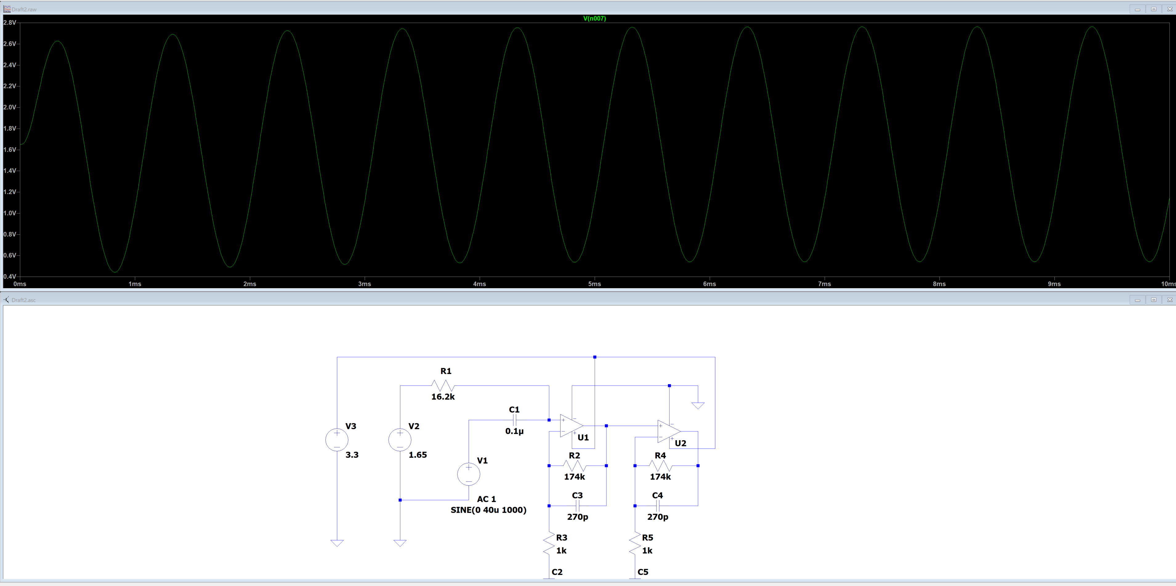 AC Analysis showing wave output from analog circuit
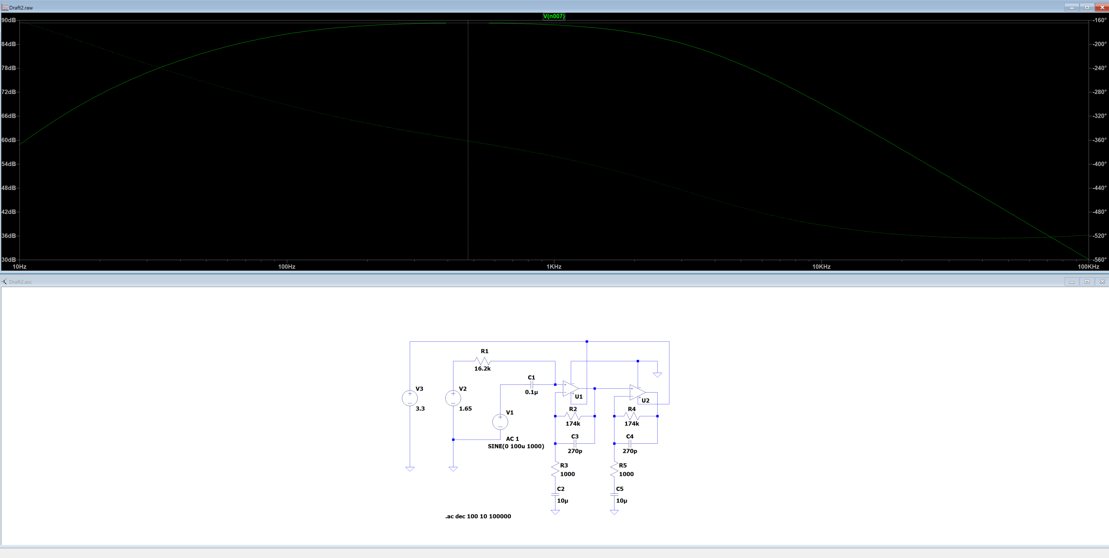 Bode plot showing filter frequency cutoffs
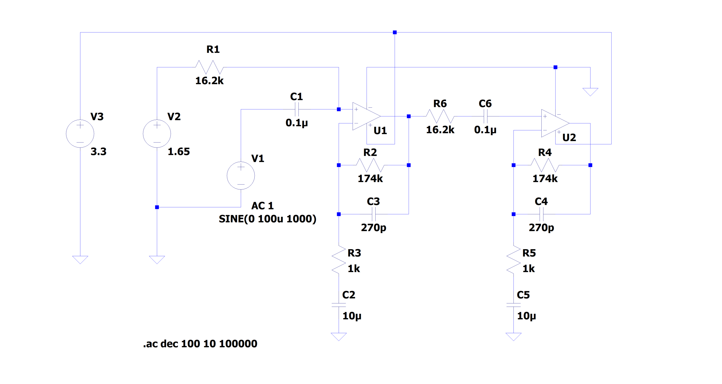 Simulated LTSpice circuit
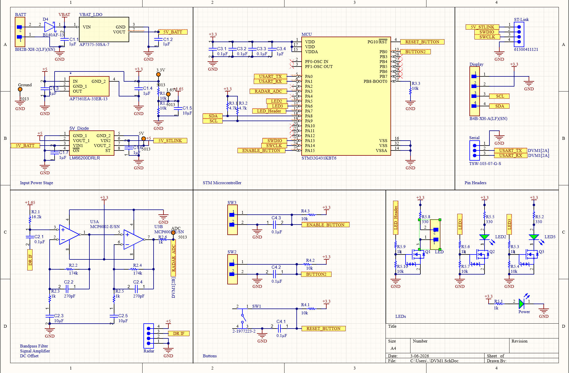 Final PCB schematic in Altium Designer
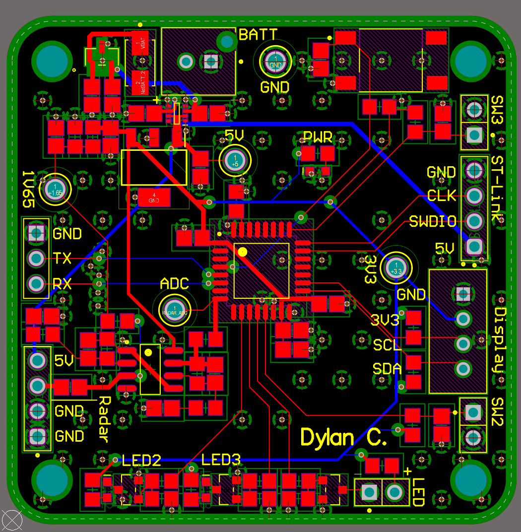
PCB Floorplanning & Signal Integrity
Drawing the schematic is only half the battle; the physical geometry of the copper dictates whether the board will actually function. I opted for a 4-layer stackup (Top Signal, Internal Ground, Internal 3.3V, Bottom Signal).
At high frequencies (like the STM32’s 170 MHz internal clock), return current takes the path of least inductance, mirroring the signal trace directly underneath it. The solid, unbroken internal Ground plane ensures pristine return paths and minimizes electromagnetic interference (EMI).
Floorplanning Architecture
- The Analog Island: The MCP6002 (SOIC-8 package) and its passive filter components are tightly clustered in the bottom-left quadrant of the board. Keeping these traces as short as possible prevents them from acting as antennas that pick up digital switching noise.
- Digital Separation: High-speed communication lines (I2C for the display, UART for telemetry) were routed to physically adjacent Alternate Function (AF) pins on the opposite side of the STM32 package, ensuring digital traces never cross into the analog domain.
- Decoupling Geometry: The
0.1 µFdecoupling capacitors were placed essentially touching the STM32’s VDD and VDDA pins. Minimizing this physical distance is critical to reducing parasitic trace inductance, ensuring the microcontroller receives instantaneous current during high-frequency clock ticks.
 Final 2D PCB routing
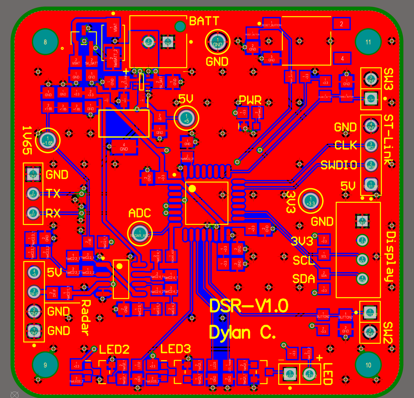 PCB top layer ground pours
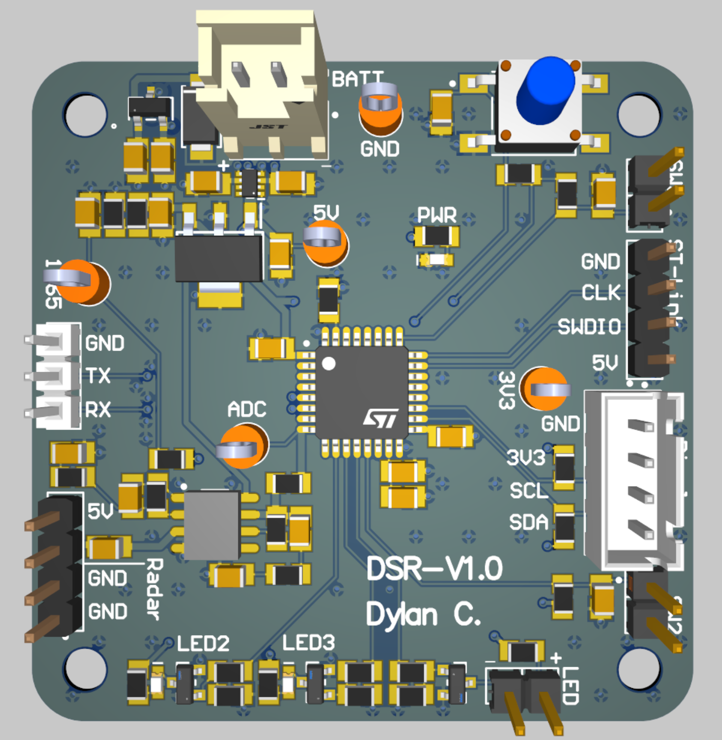 Final 3D Render in Altium Designer
Firmware & Digital Signal Processing
With the hardware outputting a clean 0-3.3V analog wave, the firmware utilizes the STM32’s high-speed ADC to sample the signal.
Example DSP Snippet
Rather than blocking the CPU to read every individual voltage point, the ADC is configured to use Direct Memory Access (DMA) to continuously fill a buffer in the background. Once the buffer is full, a fast fourier transform algorithm determines the dominant frequency.
if(data_ready_flag != 0){
					  if(data_ready_flag == 1){
						  current_buffer_ptr = &ADC_BUFFER[0];
					  }
					  if(data_ready_flag == 2){
						  current_buffer_ptr = &ADC_BUFFER[1024];
					  }
					  for(int i = 0; i < 1024; i++){
						  ADC_FLOAT[i] = (float32_t)current_buffer_ptr[i]; // Convert to float
						  ADC_FLOAT[i] -= 2048.0f; // Deal with DC offset
					  }

					  arm_rfft_fast_f32(&S, ADC_FLOAT, fft_output, 0); // Forward FFT
					  arm_cmplx_mag_f32(fft_output, fft_mag, 512); // Calculate magnitudes of the complex frequencies

					  arm_max_f32(&fft_mag[5], 512 - 5, &max_mag, &max_mag_index); // findmax

					  // Calculate the velocity
					  if(max_mag > 20000.0f) {
						  velocity = c * ((max_mag_index + 5.0f) * (10000.0f / 1024.0f)) / (2.0f * 10.525e9f);
						  velocity *= 3.6f;
					  }
					  else {
						  velocity = 0.0f;
					  }

					  data_ready_flag = 0;

					  // Scale float to maintain decimal point
					  uint16_t velocity_int = (uint16_t)(velocity * 10.0f);
Once the frequency is isolated, the firmware applies the Doppler equation to calculate velocity and pushes the formatted integer to the I2C OLED display.
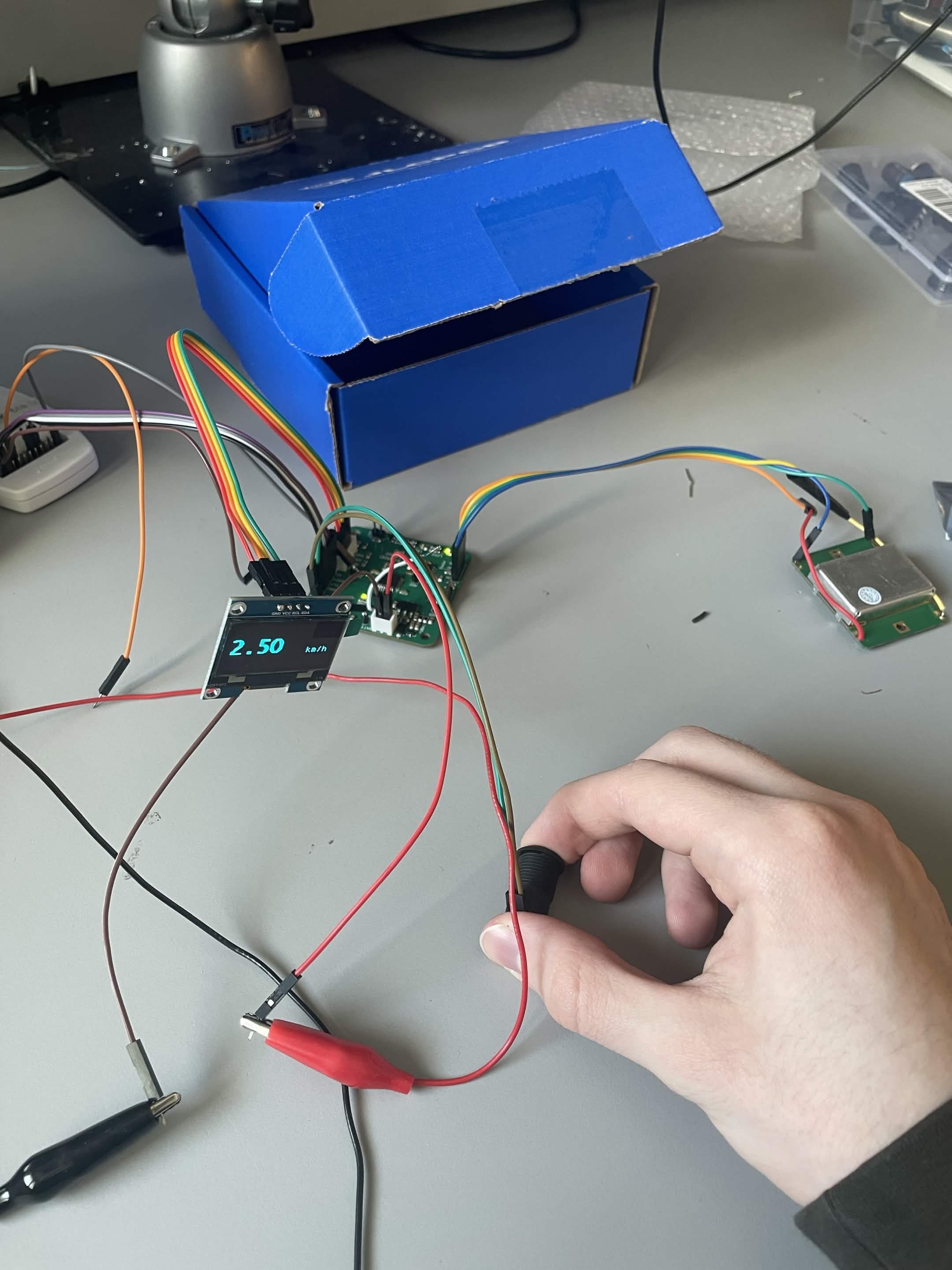 Working setup showing OLED display, PCB, radar, and pushbutton
Hardware Bring-Up & Validation
Physical testing was conducted to validate the analog and power stages before the microcontroller was programmed.
- Power Integrity: Verified the AP7375 (5V) and LP5907 (3.3V) linear regulators were outputting stable voltage under load, ensuring the battery pack’s 7.4V input was efficiently stepped down without switching noise.
- Signal Chain Staging: Used an oscilloscope to inject a test sine wave and verified the 1.65V DC offset was stable and the AC gain was accurately multiplying the signal without clipping against the rails.
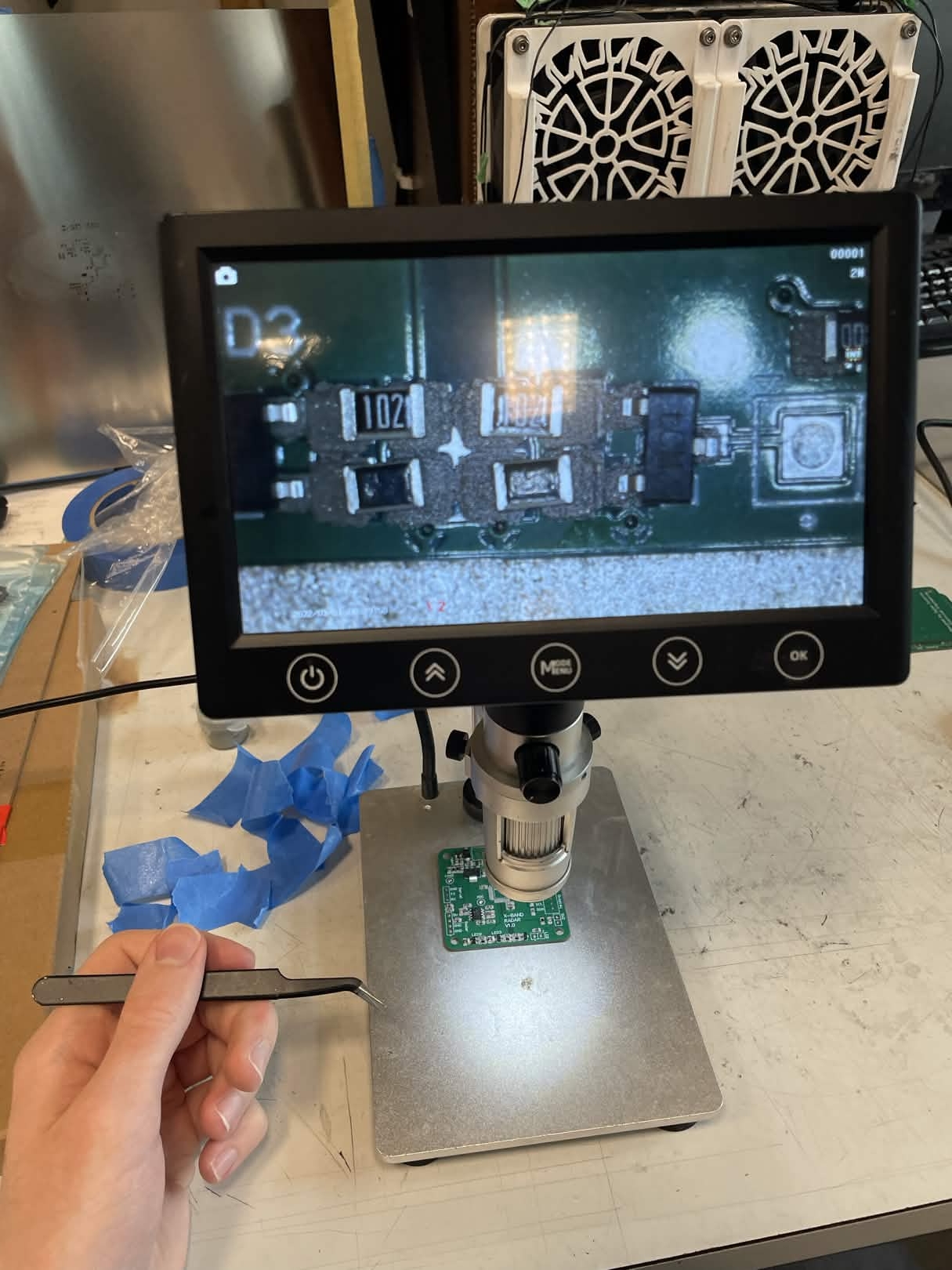 Placing SMT components during hardware bring-up
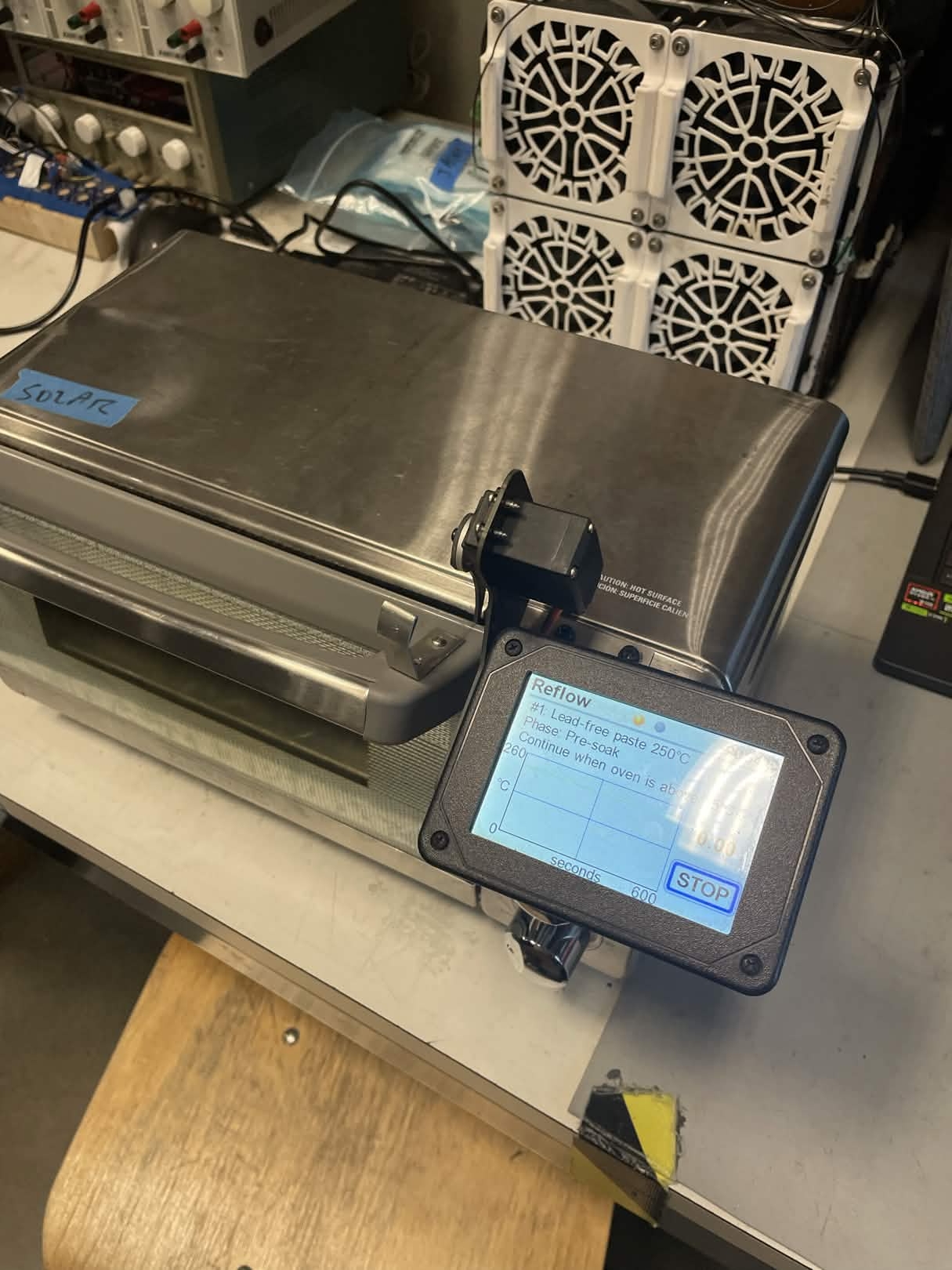 Reflowing PCB in a reflow oven
Future Revisions
While the current architecture successfully isolates the analog signal and processes velocity, future revisions of this hardware could explore:
- Active Shielding: Routing a dedicated ground guard ring around the high-impedance op-amp inputs to further suppress leakage currents and EMI.
- Moving Target Indication (MTI): Implementing a digital high-pass DC-blocking filter in firmware to aggressively reject stationary clutter (0 Hz bins) before the FFT stage, increasing the signal-to-noise ratio for moving targets.
- Gain Staging: Splitting the 175x gain across three op-amp stages rather than two to increase the overall bandwidth, allowing the radar to track objects moving at much higher velocities without attenuation.